
High-speed, high-precision model with improved usability and greater inspection compatibility for electronic components and printed circuit boards
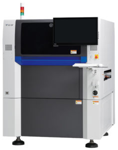
YRi-V 3D Hybrid AOI System
Yamaha Motor Europe announced today that on July 1, 2021, it will launch the YRi-V 3D hybrid automated optical inspection (AOI) system, which achieves both high speed and high precision in operation, for high-end factories mounting electronic components.
The YRi-V was developed as a higher-end version of the bestselling YSi-V 3D hybrid AOI system, which is equipped with 2D inspection, 3D inspection and a 4-direction angular camera in a single machine. By adopting a newly developed inspection head equipped with a high-speed, high-resolution camera, an updated 3D projector, a high-performance GPU and more, the YRi-V achieves the industry’s fastest inspection speed¹. Further, inspection performance has been greatly improved while building on previous levels of convenience and functionality, such as raising the inspection capabilities for fine pitch ultra-small components and detecting scratches, cracks, chipped areas and the like with mirror-surface finishes, a difficulty until now.
The main features include 1) high levels of both speed² and precision³ by adopting a newly developed inspection head equipped with a high-speed, high-resolution camera and a high-precision 8-direction 3D projector, 2) more functionality such as greater component inspection compatibility thanks to new coaxial lighting and more compatible PCB lengths via revised conveyors, and 3) improved usability thanks to using AI-powered deep learning and other changes to simplify, automate and lower skill requirements for inspection data creation, conversion, tuning, etc.
Market Background and Product Outline
The reliability shown with SMT processes directly affects the market value of the products. The SMT field in recent years has seen the shift toward smaller sizes, higher densities, greater functionality and more diversification accelerate rapidly, and in order to ensure the reliability of PCBs, fast yet precise inspection of mounting quality across all items via automated optical inspection (AOI) will be even more sought after. Also more recently, the use of thin and extremely small WLCSPs and FOWLPs⁴, which have specular gloss on the package surface, has risen significantly in the market. So, in addition to mirror-surface components that are difficult to inspect, the need for compatibility to mount ultra-small components at fine pitch is increasing.
The YRi-V accommodates these changes and demands of the market early on. This AOI system dramatically improves inspection ability in terms of both speed and accuracy, with greater detection capability for 0201 size (0.25 mm x 0.125 mm) ultra-small components and mirror-glossed components. In addition, with our unique 1-Stop Smart Solution concept, we take advantage of being the industry’s leading manufacturer with a full lineup of SMT equipment— from SMD storage, solder paste printers and glue dispensers to surface mounters and AOIs—to offer new value via the high-level integration and coordination among our line equipment that removes the need for black boxes.
Product Features
1- High speed and high precision
The newly developed inspection head features the current 12 μm and 7 μm resolution lenses as well as a new 5 μm resolution lens compatible with 0201 size ultra-small chip components. The YRi-V gains all-new lighting with increased luminance and is also equipped with the industry’s fastest high-speed, high-resolution camera with an increased frame rate. Employing a high-performance GPU yields faster image processing capabilities that achieve incredible speeds, almost twice that of the current YSi-V TypeHS2 at 7 μm and 1.6 times at 12 μm. Updating the 3D projector has also enabled even more precise inspections, with both measurement accuracy and range doubled compared to current models and high-precision measurement now possible for up to 25 mm in height. Furthermore, by combining the 5 μm lens and an 8-direction 3D projector, it is possible to perform high-precision 3D inspections of 0201 size ultra-small chip components and fine pitch components with imaging at high resolutions without the effects of component blind spots.
2- Greater functionality
The inspection head’s new coaxial lighting bolsters the capability to detect scratches, cracks and chipped areas on mirror-surface components and the detection sensitivity has also been improved. In addition, the revised conveyors expand the range of compatible PCB lengths and it is possible to flexibly handle longer, 1,200 mm PCBs (with optional fittings). In a dual-lane setup, the freer adjustability of fixed positions for rails 2, 3 and 4 have improved versatility when linking up with other equipment.
3- Improved usability
Intuitive operation is possible with the new GUI’s next-generation design. Further, automating various functions, incorporating AI and more has enabled us to offer a full range of support functions for creating inspection data and for tuning data without the need for a high skillset among operators.
During data conversion: It is possible to convert CAD/CAM/YGX data into inspection data in a single step. In addition, the machine is compatible with Gerber data as standard and automatically generates virtual board images.
When creating data: It is easier to create inspection data with features like offline data creation, individual 3D projector condition settings and automatic creation of through-hole data from raw board images.
When tuning data:
Data tuning time is halved by eliminating inspection frames (automatic calculation), automating lighting parameters and automatic position correction that accurately accounts for the degree of component misalignment. In addition, AI deep learning identifies the component type from the component image and automatically sets the ideal component library. It also greatly promotes further automation and labor saving, such as automating new component library creation and aiding with secondary visual checks and decisions.
About Yamaha Robotics SMT Section
Yamaha Surface Mount Technology (SMT) Section is a subdivision of Yamaha Motor Robotics Business Unit in Yamaha Motor Corporation. Yamaha surface mount equipment is highly acclaimed in the market for their “module concept” that enables them to keep pace with the trend toward smaller and more diverse electric/electronic parts being mounted on circuit boards.
Yamaha SMT Section has created a strong business in the surface mount industry that enables design and engineering, manufacture, sales and service to be conducted in one comprehensive system. Furthermore, the Company has used its core technologies in the areas of servo-motor control and image recognition technology for vision (camera) systems to develop solder paste printers, 3D solder paste inspection, 3D PCB inspection machines, flip chip hybrid placers, dispensers and intelligent SMD storage system. This allows Yamaha SMT Section to offer a full line of machines for electric/electronic parts mounting and propose optimum production-line makeup to answer the diversifying needs of today’s manufacturers.
Yamaha SMT Section has sales and service offices in Japan, China, Southeast Asia, Europe and North America provide a truly global sales and service network that will safeguard best in class on-site sales & service support for clients.
____________________________________________________________________________________________
1 According to Yamaha Motor research as of May 19, 2021.
2 When imaging with 4 projectors vs. the current YSi-V TypeHS2 model, the YRi-V’s inspection speed (mm2/s) is about 1.6 times faster at 12 μm resolution and about 2 times faster at 7 μm resolution.
3 Approximately twice the repeatability of the current YSi-V TypeHS2 model when measuring the height of chip components.
4 WLCSP = Wafer Level Chip Size Package FOWLP = Fan Out Wafer Level Package