
Measuring just 0.25mm x 0.125mm, the agreed industry standard, these tiny devices are just over half the size of the 0402 (0.4mm x 0.2mm) form factor. Their arrival on SMT assembly lines challenges printing, mounting, and inspection processes to increase accuracy and maintain speed. The first article in this series of two suggests improvements in the screen printing process.
Stencil-to-Board Gap
An accurate, repeatable print process is the cornerstone of high-quality surface-mount assembly. Getting the process settings absolutely correct will become more important than ever as 0201mm devices enter widespread use. Studies have shown that ensuring a reliable seal or gasket between the stencil and PCB, as well as optimising aperture fill and ensuring efficient paste release after separation, have a powerful influence over the process yield.
To establish a good enough seal, the maximum acceptable stencil-to-board gap is only 0.2mm. This limit becomes more critical than ever, when printing for 0201mm. Figure 1 presents statistical analysis of paste-volume repeatability at an aperture size of 0.22mm x 0.24mm, showing how repeatability deteriorates rapidly as the stencil-to-board gap exceeds 0.2mm.
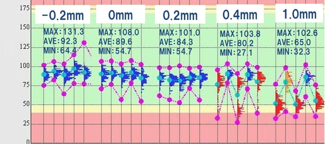
Figure 1. Stencil-to-board gap greater than 0.2mm compromises printing
Aperture Filling
With extremely small stencil aperture sizes, optimum filling efficient paste transfer after separation are critical.
The squeegee angle is known to influence aperture filling more heavily than squeegee pressure, and must be reduced as the paste roll diminishes. Experiment shows that the squeegee angle should change from about 60 degrees to 50 degrees before paste is replenished. Yamaha’s servo-controlled 3S (Swing Single Squeegee) head for YSP printers automatically re-adjusts the squeegee angle on each cycle.
The smaller 0201mm aperture area means solder-paste particle size also becomes more critical. Currently, Type-3 and Type-4 pastes, with typical particle size of 30μm and 35μm, are used in general SMT assembly. Type-5 (20μm) pastes produce better results when printing for 0402mm chip-size parts, but are more expensive.
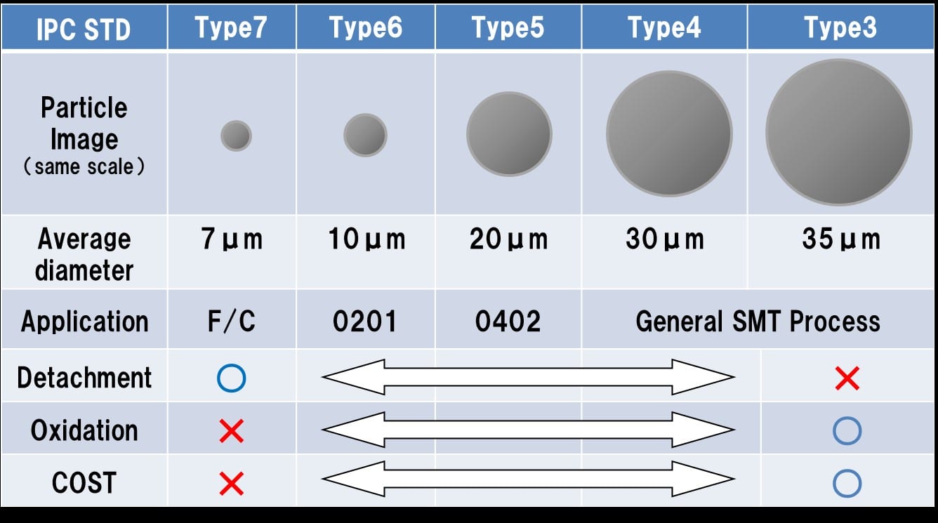
Table 1. Paste types and major parameters.
Stencil Thickness
Stencil design has focused for many years on aspect ratio (aperture width ÷ stencil thickness) to achieve the best possible filling and transfer. A rule of thumb has specified a minimum ratio of 1.5, indicating that reducing aperture sizes demands an associated reduction in stencil thickness. More recently, the area ratio (bottom area ÷ lateral area) has become a widely used metric and experts have suggested a ratio of 0.6 or even 0.4 for the latest chip-size parts.
To satisfy either of these formulas, the contact area of the pad must be greater than the total area of the aperture wall. Effectively, the stencil thickness must be reduced to ensure satisfactory paste release at smaller aperture sizes. Table 2 summarises the typical ranges of stencil thickness, in relation to SMD chip-component sizes.
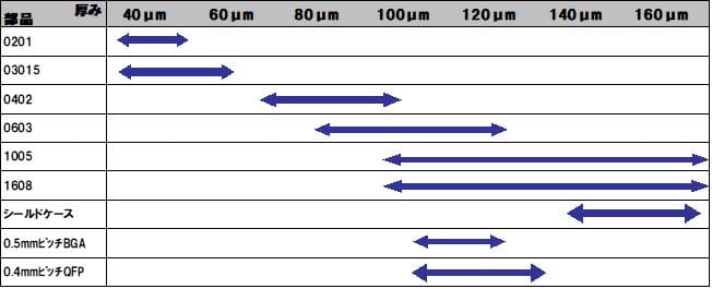
Table 2. Typical optimum stencil thickness for component sizes down to 0201mm.
Sequential Printing
A stencil thin enough to print the minute volumes of paste for the smallest-size 0201mm pads will be unable to deposit adequate volume for larger parts. Stepped stencils have delivered limited success in overcoming similar, less severe, challenges in the past. Solder preforms can be placed where large volumes are required, but are expensive and impose additional placement burden.
Yamaha has proposed two-stage sequential printing as a suitable solution. The smallest deposits are printed first, using the thinnest stencil. A thicker stencil is subsequently used to deposit larger paste volumes where required. The underside is routed to prevent contact with the existing solder deposits. A dual-lane printer with sequential printing mode, such as the Yamaha YSP20, is needed.
An additional benefit of sequential printing is the opportunity to reduce the solder-paste cost per board by using the more expensive type 5.5 or 6 paste for printing fine features only. A coarser particle size can be used for depositing larger volumes of paste. Figure 2 shows print deposits for 0201mm SMD devices and larger components, created using two-stage sequential printing.
About Yamaha Robotics SMT Section
Yamaha Surface Mount Technology (SMT) Section is a subdivision of Yamaha Motor Robotics Business Unit in Yamaha Motor Corporation. Yamaha surface mount equipment is highly acclaimed in the market for their “module concept” that enables them to keep pace with the trend toward smaller and more diverse electric/electronic parts being mounted on circuit boards.Yamaha SMT Section has created a strong business in the surface mount industry that enables design and engineering, manufacture, sales and service to be conducted in one comprehensive system. Furthermore, the Company has used its core technologies in the areas of servo-motor control and image recognition technology for vision (camera) systems to develop solder paste printers, 3D solder paste inspection, 3D PCB inspection machines, flip chip hybrid placers and dispensers. This allows Yamaha SMT Section to offer a full line of machines for electric/electronic parts mounting and propose optimum production-line makeup to answer the diversifying needs of today’s manufacturers.
Yamaha SMT Section has sales and service offices in Japan, China, Southeast Asia, Europe and North America provide a truly global sales and service network that will safeguard best in class on-site sales & service support for clients.
www.yamaha-motor-im.eu
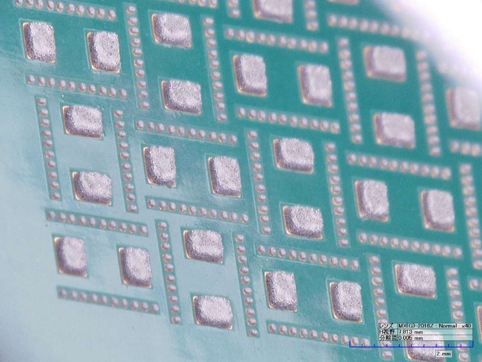
Figure 2. Large-volume and ultra-small paste deposits created using two-stage printing.
Contact info
Oumayma Grad
Marketing Communications Manager
Hansemannstraße 12
41468 Neuss
Germany
Office: +49 2131 2013 538
Mobile: +49 1517 0233 297
Fax: +49 2131 2013 550
Email: oumayma.grad@yamaha-motor.de
Web: www.yamaha-motor-im.eu